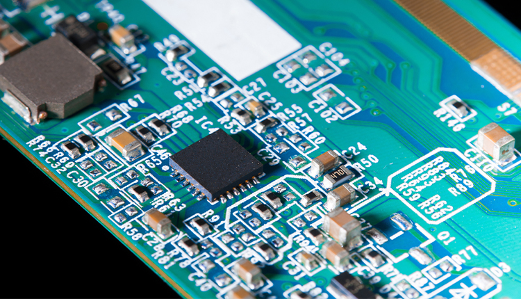


As the main process to ensure the reliability and stability of product quality in the electronics industry, the thickness of the coating is the most important guarantee factor for product quality. Therefore, the quality control/guarantee of the thickness of the coating is very important.
X-ray fluorescence (XRF) has become a widely used technique for coating thickness and composition measurement because of its non-destructive, fast measurement, and ease of use.
INSIGHT aims to provide accurate and efficient analysis methods for coating analysis applications.INSIGHT is easy to operate and flexible to configure, which can easily challenge ultra-thin coatings, provide fast, accurate and repeatable results, and help many PCB, semiconductor and other electronics related industries effectively improve productivity. And it ensures compliance to specifications to avoid the risk of poor performance and costs associated with scrap or rework. and it ensures compliance to specifications to avoid the risk of poor performance and costs associated with scrap or rework.

Printed Circuit Boards
Au/Ni/Cu/PCB;Sn/Cu/PCB;Au/NiP/Cu/PCB;Ag/Cu/PCB;Sn/Cu/PCB;SnPd/Cu/PCB;Au/Pd/NiP/Cu/PCB
Connector Plating
In the electronics and electrical industry, the use of protective and wear-resistant coatings for electrical contacts is increasing. As the core component of the electrical connector, the surface treatment can improve the corrosion resistance and wear resistance of the contact, and can also optimize the transmission function of the contact to a large extent. The base material of electrical connector contacts is generally copper alloy, and the commonly used plating layers are: tin plating, gold plating, silver plating, nickel plating, palladium plating, etc.
Wafer Manufacturing (Semiconductor)
Wafer refers to the silicon wafer used in the fabrication of silicon semiconductor integrated circuits. In the production process, the wafer needs to be electroplated, that is, a layer of conductive metal is electroplated on the wafer, and the conductive metal layer is subsequently processed to form a conductive circuit. As the basic material of the chip, the wafer has strict requirements on the electroplating layer, so the process requirements are also high. During wafer plating, the uniformity and thickness of the coating must ensure the quality of the wafer.
| The characteristics of | Top-down measurement structure, XYZ measurement platform, MUTI-FP multilayer algorithm |
| Scope of element | Na(11)—Fm(100) |
| Analysis of the layer number of | 5 layers (4 layers + substrate) each layer can analyze 10 elements, composition analysis can analyze up to 25 elements |
| X-ray tube | 50 W (50 kV, 1mA) micro-focused tungsten palladium ray tube (target material is optional) |
| The detector | High sensitivity large area SDD detector, SDD 50mm2 large area detector, (optional) |
| Collimator | Multiple collimators are optional, and multiple collimators can be combined |
| The camera | High resolution CMOS color camera, 5 megapixels |
| magnification | 40x-160x |
| Manual sample XY platform | Moving range:100 x 150 mm |
| Programmable XY platform | (Optional) |
| Z-axis range of movement | 150 mm |
| Sample bin size | 520 x 480 x 170 mm (L x W x H) |
| Overall dimensions | 624 x 702 x 730 mm (L x W x H) |
| weight | 120KG |
| The power supply | AC 220V±5V 50Hz(The configuration varies slightly by region) |
| Rated power | 150W |